PCBA (Printed Circuit Board Assembly) manufacturing is a critical process in the production of electronic devices, encompassing the assembly of components onto a printed circuit board. This article delves into the various stages involved in pcba manufacturing, highlighting the key steps and considerations.
1. Design Phase
PCBA manufacturing begins with the design phase, where the circuit board’s layout is created using specialized software. This design includes placing components and tracing the electrical connections between them. Design considerations include:
- Component Selection: Choosing appropriate components based on functionality, cost, and availability.
- Layout Design: Arranging components to optimize space and signal integrity.
- Electrical Design: Ensuring electrical connections meet performance and safety standards.
2. Manufacturing Preparation
Once the design is finalized, the manufacturing process prepares for PCB fabrication and component procurement:
- PCB Fabrication: The circuit board is fabricated based on the design specifications. This involves laminating a layer of copper onto a non-conductive substrate and etching away excess copper to form the circuit paths.
- Component Procurement: Sourcing the required electronic components from suppliers, ensuring they meet quality standards and are compatible with the design.
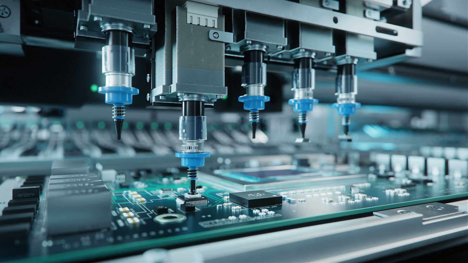
3. PCB Assembly
The PCB assembly process involves populating the circuit board with electronic components:
- Solder Paste Application: Applying solder paste to the PCB, which will hold the components in place during soldering.
- Component Placement: Automated machines or technicians place the components onto the board with precision.
- Reflow Soldering: Heating the board in a reflow oven to melt the solder paste, permanently attaching the components to the PCB.
- Inspection: Automated optical inspection (AOI) or visual inspection checks for defects like misalignment or soldering issues.
4. Testing and Quality Control
After assembly, rigorous testing ensures the PCB functions correctly:
- Functional Testing: Testing the board to ensure it operates according to specifications.
- In-Circuit Testing (ICT): Testing individual components and circuit paths for faults.
- Quality Control: Inspecting for physical defects and verifying compliance with standards.
5. Packaging and Shipping
Once tested and approved, PCBAs are prepared for shipping:
- Packaging: PCBAs are packaged to protect them during transportation and handling.
- Shipping: Distributing to customers or further stages in product manufacturing.
6. Environmental Considerations
PCBA manufacturing must consider environmental impact:
- Materials: Using environmentally friendly materials and processes where possible.
- Waste Management: Proper disposal or recycling of waste materials.
7. Technological Advancements
Recent advancements in PCBA manufacturing include:
- Miniaturization: Smaller components and tighter packing densities.
- Automation: Increasing use of robotics and AI for assembly and inspection.
- Green Manufacturing: Eco-friendly practices and materials.
PCBA manufacturing is a complex process that integrates design, fabrication, assembly, and testing to produce high-quality electronic devices. Advancements in technology continue to streamline the process and improve product reliability, contributing to the growing demand for electronic products worldwide.